Tuesday, March 29, 2011

CIRCUIT ONE ( BIPOLAR JUNCTION TRANSISTOR CIRCUIT)

I have for this circuit: Vs= 12V, two LEDs 1.8V (20mA)      Ic = 20mA

Caculation for R14 &R15:
R = Vs - VLed - Vce / Ic   ( R = 12Vs - 1.80V Led - 0.2Vce / 0.02A Ic= 500 ohms
R14 & R 15 = 500 ohms.
Ib = from data sheet ( Ic = 10mA =0.5mA)
Ic = 20 mA , Ib = 1mA (sat)
B = 110 from the data sheet
Ib = Ic / B  0.02A/ 110 = Ib 0.00018A
R13, 16 = Vb - Vbe / Ib   ( 5V - 0.7V / 0.00018A = 2388 ohms (2.4K ohms)
R13,16 = 2.4 K ohms
The current Ib is low and high risistor in this stage transistor is not saturated , lets find other risistor for Rb.
Vbe (sat) Ic = 10mA , Ib = 0.5mA or Ic = 100mA , Ib= 5mA ( from data sheet)
Ic = 20mA , Ib = 5mA   (from data sheet)
Rb13,16 = Vb - Vbe / Ib   ( 5V - 0.7V / 0.005 = 860 ohms
Rb 13 & 16 = 860 ohms

Saturation: Rb = 5V- 0.7V / 0.005A= 860 ohms
Active ( current gain ); Ib = Ic / B
Rc = Vcc - Vled - vce / Ic  ( 12v - 1.8 v - 0.2v / 0.002A = 500 ohms)

Summary;
Vs = 12V
Led= 1.8V
Vce= 0.2V
Ic = 20mA
R14, 15 = 500 ohms
Vb = 5V
Ib = 5mA
Rb 13, 16 = 860 ohms
Vbe = 0.7V

Next step start to disigened the circuit on Loc Master 03


I have start to build the circuit;
Componint : two C577 transistor, two 1.8v LEDs, two 1Kohms risistors, two 680 ohms risstors & circuit bord.

This is a bipolar junction transitor circuit consist of two LEDs in parallel, four roistors, and two transistors which i will be focusing on there functions. BJT has three terminal electronic divice constracted of dope semiconductor materialwhich is using in switching applications.
This BJT circuit needs only 5V to switch a 20mA lamp it means that this 5V Will go trogh base to emitter to open the gates for Vcewich is higher voltage to cause the signal or the LED to flash and this process take place in Active Region of the transistor, Normally transistor has three regions.
1) Active Region; where power dissipation is very high.
2) Satuaration Region ; with both junction forward biase, BJT saturation mode facilites high current conduction from emetter to the collecor which is closed switch.
3) Cut off Region: This is the opposiite to saturation , both junction are revers bias there is very little current flow  which corresponds to an open switch.
The easy and more effecint way to find the three region and calculate the current gain is the graph of Vce, Vs , Ic for diffrent level of Ib  and the common emetter circuit B (Beta) which is ratio between collector current and base current and represinting in B = Ic / Ib
The two pulsing terminal which are only 5V going throgh base to emitter (Vbe) and this will open the gate for the collector to emitter (Vce) .

TEST:

Test
Suppling 12V to the circiut with two terminals connected to the 5V supplay for the open gates of the VCE.
Checked avaliable voltage in varios points and the ressults were positive, checked available voltage after R15= 11.38V, voltage drope led 2 2V , voltage drope vce 0.74v, voltage drope bce 0.72v , voltage drope between R15 to colector 6.20V, LED1 voltage drope 1.90V, transistor2 be 0.70V.
testing of this circiut gave me positve result because switching the transistor voltage 0.6v - 0.70V and the Led s on ad brightness . i can say if the vbe is less the the current cant flow to emmiter and the LEDs of this circuit shuld not brightt,.
Reflection:
I made this circuit sample and easey i follow the instruction and also i had no diffeculty in this circuit just only i had connect one of resistor in wrong place than i noticed quuik unsoldred and put on right place .
next time i hope i would make batter than this circuit.

Wednesday, March 23, 2011

EXPERMENT NO.8

. Use a Set up the following circuit on bred board470 R for Rc and a BC547 transistor.

In this circuit i used five resistors for Rb. 1M, 47K, 220K, 270K & 330K ohms. Why we doing that , because change the risitors we see when the transistor saturated switch rigion and when is active amplifier region. Also i had record voltage drop across Vce & Vbe & recorded the current for Ic & Ib.
Every change the risitor for Rb i have measure & recorded in below chart.

Rb 270K    Vbe: 0.66V       Vce: 1.73V         Ib: 0.02mA        Ic: 0.425mA
Rb 47K      Vbe: 0.67V       Vce: 0.72V         Ib: 0.10mA        Ic: 4.38mA
Rb 2.2K      Vbe: 0.70V       Vce: 0.16V        Ib: 1.97mA        Ic: 4.46mA
Rb 1M        Vbe: 0.63V       Vce: 2.25V        Ib: 0.01mA        Ic: 0.02mA
Rb 330K     Vbe: 0.66V       Vce: 0.25V        Ib: 0.02mA        Ic: 4.13mA

Let see some of my experiment pictures, I had take of every measarment that,s too much just afew i will put in this blogg.
In this picture voltage drop across Vbe, for Rb 270K.


Mesurment of current Ic, Rb 47K ohms in circuit.


   In this picture measuring current flow Ib for Rb 47K.


Measuring Voltage drop a cross Vce for Rb 1M in the circuit.


In this picture measuring current of Ic, Rb 330K ohms in the circuit.

Now discussing what happed for Vce during expeeriment & what caused of change.
In this circuit i had used diffrent resistor the big risistor on Rb Voltage a cross Vce is high small risistor voltage drop Vce is low. We can see when high voltge drop on Vce this cauuse we have put big risstor on Base that way high risstnce on base means less current flowing on base (Ib) and Ic is also low current. In this stage the transitor in cutt off or active region not saturatioin region, because not enough current for Ib to switch on of transisor. The small risistor voltage drop across Vce is low and the current Ib is high and also the curret of Ic is also high in this the transistor is the saturarated region.
If we see on record on top the smallest risistor i used in this circuit in Rb is 2.2K ohms the Vce is 0.16V , Ib 1.97mA & Ic 4.46mA that is the transistor is saturated region fully swith on , because more current flowing on base. The voltage drop across Vce from below 0.3V transistor is in saturaed region and above 2.0V transistor is in active region.

Discuss what happened for Vbe during this experiment . What change took place, if any and what caused the change?
The voltage drop in Vbe in this circuit not changed in any diffrent risistor, because transistors are designed two diode back to back voltge drop Vbe sammelar like normal diode.Also risistor only control the current not voltage taht way changing the risistor only change the current flow Ib & Ic voltage drop Vbe is same.
We allways in our calculation voltage drop Vbe is 0.7V.
For example: if we want to find the valve of risitor Rb incircuit we used this formulla.
Rb= Vb - Vbe / Ib  (Rb= 5v -0.7Vbe /Ib).

Discuss what happened for Ib duuring in this experiment. What took place, and what caused the change     
During this experiment current Ib is changing the cause of cahnging Ib is risistor high risstance on base less current flow to base to emitter and Ic is also low. The big risistor on circuit voltage drop a cross the Vce is high means high voltage dorop on Vce that way we can get less current on base, Also in less current or not enough current the transistor is cutt off rigion or active region. Small risistor current Ib is high and vce is low transistor is saturated.

Discuss what happened for Ic during this experement. what change took place , and what caused the change?
Ic current flow to collector is also related to risistor, high risitance more current . In this circuit i have noticed high voltage drop across vce get less curent Ic . When i used a small ristor on base we can get more current in Ib .When Vce is less the Ib is high .If we lock the plot the Vce geting smaller Ic is going up and also the Ib and transitor is saturated . You can see difrence of Ic in ristor in my measarment rrecod .

Calculate the Beta (Hfe) of this transistor.
B= IC/Ib     B= 0.425/Ib 0.02mA= 21.25  OR (Ib= IC/Ib  0.425mA/B21.25= Ib 0.02mA
                 B= IC4.38mA/Ib0.10mA= B 43.8   OR (Ic4.38mA/B43.8= Ib 0.10)
                 B= Ic4.46mA/ Ib 1.97= B 22
                 B= Ic0.002A / Ib 001A = B 20
                 B =Ic 0.o413A / Ib 0.002A = B 20.65

Explain what the load line graph is telling you.. Discuss the region of graph where the transistor is Saturated, cut off, or in the Active area.

The load line the graph is telling cut off and saturated region. the end of the load from Ic to is the large supplay voltage , if the saturated area when the base current has incresed The emmeter base junction is forward biase infact if the base current it can cause Ic current flow to increase.
In saturation the transistor
Volt 0- 0.2V
Vce<=0.2V tis knew the saturate volt or Vce(sat)
Ib >0.and Ic >0
Vbe>= 0.7V
Cutt off region the transisor inaactive. In the cutt off the following behave is noted
Ib = 0 (no base current)
Ic = 0 (no collecor emmeter )
Vbe = 0.7V (emetter , base junction is not forward)
Active region the transistor can act as fairly liner amplipir in this region
0.2V>Vce<Vce
Ib>0 and Ic>0
Vbc> = 0.7V
The transistor in ON and  the collector to emetter voltage is some where between the cutt off and saturated stage. this the transistor is able to amplyfy smalll voltage present to the base the act is extracted if the collector in forward active stage the collector current is proprtional to the base current by a constant multiplir Beta (Ic= B* Ib).
0

Sunday, March 20, 2011

EXPERMENT NO. 7 Transistor as aseitch

Componints; 1 * Small signal NPN transistor, 2 resistors.
Exercise; Connect the circuit  Vs 15V, R1= 10K ohms, R2 = 1K ohms

I had build this circuit and used 1 * 1K ohms, 1 * 10K ohms transistor, 1 * PNP(C557) transistor and 15Vs.
Connect the multimeter between base and emitter.
Note the voltage reading reading and explain what this reading is indicating.

The voltage drop between base and emitter in my test 0.78V.
The voltage drop across the base to emitter junction is also called in datasheet Vbe, this also for silicon transistor 0.6V to 0.7V is the valve of the voltage drop.
If we calcullate the current that will flow in the base must subtract this valve from the total voltage.
for example: We have in this circiut 15Vs the voltage across the R1 = 14.2V (15Vs - 14.2 - 0.7=0
Vcc=IC*Rc+Vce or Vcc- Ic * Rc - Vce =0.

Connect the meter beteween collector and emitter .
Note the voltage reading and explain wwhat this reading is indicating


The voltage drop between collector and emiter is 55.8 mv.
The voltage drop between collector and emetter even is saturated means not perfect conducter. This voltage is also call Vce (sat). BJT two transistor connect back to back . If the transistor saturated voltge .55v in this circuit the current that mean the current will fully switch on Vs - Vce / R.

In the plot given below what are the regions indicated by the arrows A &B?

Arrow A is SATURATION region in this region emitter and collector are in forward biased , which is the Vce is will be zero and the supplay volatage will be across the load means ON .

Arrow B is represiting CUTOFF region the emitter and collector junction are be in reverse bisssed , and this region the current Ib is zero and the collector current will not fllowing. means (OFF)
Cutoff and saturation regions the miniumum power dissipation of transistor are :
Furmulla: PD=Vce * Ic  in both regions Vce are =0 then the Pd = 0 if we flow  the ohms law P=VI.

What is the power dissipated by the transistor at Vce of 3V?

P= IV
Pd = Vce * Ic
Pd = 3Vce * 14Ic = 42mW( 4.2W)

What is the Beta of this transistor at VCe 2, 3 and 4 Volts?

B= IC / Ib
Vce2, B= Ic/Ib   20Ic/0.8Ib = B25
Vce3, B = Ic/Ib   14Ic/0.5Ib = B28
Vce4, B = Ic/Ib    5Ic/0.2Ib = B25

Friday, March 18, 2011

EXPERMENT NO. 6 Meter check of transistor

Meter Check of Transistor

In this experment i'd explain how can check the Bipolar Junction Transistor (BJT).
BJT transistor three layer semiconductor two type PNP or NPN these like two diodes connected back to back. When we testing with a multimeter with diode function. How can identify PNP or NPN? Low voltge reading meter with the negative (-) leads that is the N type transistor which is PNP transistor .
low voltagereading with positve(+) lead on base wich opposite of NPN.

The thyory of BJT
Transisor are current controled soled state divices, that cunduct current in proportin to an inpt current .
The symbol of BJT PNP & NPN transsitors are bellow;
For the NPN transistor, current flowing into into base (B) of transistor the resullt in proportionally a large current to flowing between collector (C) & emitter (E).
The curent flowing out of base PNP transistor alows propoortional current to flow between the (E) & (C).

BJT terminal identified by meter.
I have got two BjT NPN &PNP for identifing legs of transistor used my multi meter on diode function, and folow instruction my work book page 18 .
The meter reading recoord in below chart, also the pictures you can see reading.

Diode test with meter reading.

Transistor
Number
V BE
V EB
V BC
VCB
V CE
V EC
NPN (C547)
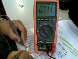
0.711 v
0.716v
0.715 v
OL
OL
OL
PNP (C557)
OL
OL
0.712 v
0.718
OL
OL


                  testing NPN (BJT) (C547) V EB =0.16v forward


              Testing BJT NPN , V CB reading OL


                      testing , BJT, NPN, V CE OL


                            testing BJT, NPN, VBE 0.711


                        Testing BJT ,PNP VBC 0.712

             testing BJT (C547), NPN, VCE (OL) 
        TEsting BJT(C547) NPN, Veb 0.16

                 Testing BJT (C557) Vbe OL


                    Testing BJT (C547) NPN , Vbc 0.17


                             Testing BJT (C557) PNP Veb OL


In this i have find wich terminal of risistor are collector, base and emitter.
the first thiing i notesed meter reading only between two terminl of ristor . The reading between emitter to base in my reading 0.7V that should in forward biase, which is NPN (BJT). Also collector to base in PNP 0.71v i had recorded .These reading also idintify me wich is PNP or NPN because , current flowing from emitter to base on PNP current can not flkowing  from base or collector to emitter, and in NPN current flowing from base to emitter, also we can say in forward biase.
                 

EXPERMENT NO. 5 ( The Capacitor)

Capacitor

First i would like write some about capcitor:
Capacitors are componint that are used to store electrical charge in used in circuit. Capacitor can be used with risstor to preduce a. some that capacitor used to smooth a current in the circuit, that can prevent false trigger of other component, suh as really
when the power supplay to the circiut that induced a capacitor. The capacitor caharge up when power is turend off and the capacitor discharges it is electrical charge slowlly.

Acapcitor is composed of two conductors sepretelly lay an issulation matireal called (Dielectric). That can be paper, plastic film, cermic, air or vacuim.the plate can be almunium disc, almunium foil or then film of metal appled of opposit side.the p;ate is negative and positve, these capacitor called (electrolyte capcitor) polarised wich mens they have (posiitve ) and (negative ) leads must be in acircuit in right way.
The other type is non elctrolyte the have a lower capacitance they are not polorise , do not have positve and negative leads can be placed anywayin the circuit. They are used normmally  to smooth current in the ciirciut.
                                                           ( Non electolyte capacior)
Capitor charging Circuit
Componints: 1 * resistor, 1 * capacitor , 1 push button switch.
In this exersise i used diffrent size of resistors and capacitors. first i had calculation and used they in serise circuit and measured time on oscilloscope and recorded in the chart beloow .


Circuit
number
Capacitance
       (uF)
Resistance
   (   K ohms)
Calculated 
Time (ms)
Observed
Time (ms)
            1
        100
         1
          500 (ms)
   470 (ms)
            2
        100
        0.1
          50   (ms)
     70 (ms)
            3
        100
        0.47
          235 (ms)
    200 (ms)
            4
        330
          1
           1.65 (s)
    175 (ms)

Calculation: The time depends on the ristance and capacitance (RC) in a circuit, the time constance can be calculated using uquation
T= RC
T= time in second
R= resistance in ohms
C= capacitancein frads
After 5 time constance a capacitor will be fully charging, there for the charging time of capacitor equal 5time the time connstance.
we used this formula (R*C*5=)

Connect of capacitor:
In series , work the opposit to risistors and the overal of valve of capcitor will rediuce. the formula to calculate total capacitor in serius     1/CT= 1/C1+1C2+1/C3
I n parallel, when capcitor connected the result the sum of all capacitors.
formula ;  CT = C1+C2+C3

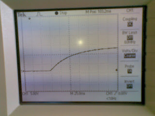
Now i made a cicuit wich is 12Vs resistor and capacitor, i have used in that circuit diffrent size of resistor and capacitors,and measured time by used oscillscope. the observed time i recrded in chart up , and next some pictures shows wayform on oscvillocope.

Cicuit 1                             CH1     5V per division        time: 50ms per division
Capacitance: 100uF      Resistance: 1Kohms


Circuit: 2                       CH1             5V per division          time; 10ms per division
Capacitance; 100uF           Resistance: 100 ohms


Circuit ; 3                       5 V per division                    time: 25ms per division
Capacitance: 100uF              Resistance 447 0hms

Circuit 4                       5V per division                  time 25ms
Capacitance: 330uF                  Resistance: 1K ohms

How does change in the resistor affect the charging time/
If we look my calculation and obsevation time we can notice the big resistor take more charging time to charge the capacitor, and also the big capacitor has get more time to charge but store charging time is longer then small.

How does charging in the capacitor affect the chargingtime?
When the the circiut switch on the capcitor charge up when switch turned off elctricty stor for few seconds in the capacitor. the capacitor discharge slowlly . if resistor intruduce to the circuit the capacitor charge more up slowlly but also discharge slowlly
Bellow graph of chargin and discharging.
                  

Thursday, March 17, 2011

EXPERMENT NO. 4

Componints: 1 * resistor, 1 *5V1 400mW Zener diode, 1 *Diode 1N4007.

Vs= 10 & 15V, R= 1Kohms

                                             10 Volts                                                      15 Volts
Volt drop V1:                        4.63V                                                    4.80V
Volt drop V2:                        0.63V                                                    0.66V
Volt drop V3:                        5.26V                                                    5.47V
Volt drop V4:                        4.73V                                                    9.54V
 
Calculate current A:     4.74A                                                     9.54A
I= Vs - V1(ZdV)+V3(DV) / R.
I= 10V - 4.6V + 0.63V / 1 Kohms=4.74 A                       I=15V - 4.80+ 0.66V / 1Kohms=9.54A
I=4.54A                                                                             I= 9.54A

There are some pictures of my experement.
Discribe what is happining and why you are geting these reading?

In this circuit i put 1* Zener diode on reverse biase and on diode on forward biase. The zener diode on forward biase on circuit working same normal diode , but onreverse biase depend on diode voltge. This zener diode is 5v in this reading we can see wich (V1) is zener diiode on reverse the voltage drop is 4.63V, that way for the safe region voltage throgh on diode in reverse biase up to 5V.
The other diiode wich is 1N400 in forward biase in this circuit the votge drop is normally 0.6V to 0.7V. In my reading is on 10Vs voltge drop 0.63V & 15Vs is Vd 0.66V. If we see between 15Vs & 10V diffrence voltge drop acrross the diodes noot toomuch littile bit , And also i had current calculation from my reading. I had got correct reading in this experemint.

Wednesday, March 16, 2011

EXPERMENT NO. 3

Componints: 2*resistor, 1* 5V 1 400mW Zener diode (ZD).
Exercise;

For R = 100 ohms & RL = 100 ohms, Vs 12V.

I= V/R
IL = Z v/ RL
IL= 5zd V/ 100ohms =50 MA (IL=50MA)
IS= Iz+ IL   (Iz= 80MA from data sheet)
IS = 80MA+ 50MA= 130 MA
Is = 130 MA
R= Vs - Vz/ I
R= 12 Vs - 5vz/ 130 MA=538 Ohms
R=538 ohms


What is the valve of Vz?  5V
Vary Vs from 10 V to 15V
What is the valve of Vz?
10Vs = Vz =4.70 V
15 Vs= Vz =5.9V           (these reading you can see on picture whiche are measure with multimeter)


Explane what is happening here.
When i change from 10 V to 15V there was littile diffrent voltage drop on zener diode . On 15Vs zener diode voltage drop 5.9V & 10Vs voltage drop 4.9V.

This circuit could be used for voltge regulator.

What is the valve of Vz? Make a short comment why you had that reading?
The valve of this  Vz is 5V. why i had that reading , because the forward biase region zener diod the same characteritic as normal diode, but the revese charactertic voltage regulator. In this circuit i had used the zener diode on revevese biase voltage cross trhogh up to or little more then 5V, which my reading on 15Vs to 5.9v, Also the Zener diode has diffrent level of breakdown voltage reverse biase region.

Tuesday, March 15, 2011

EXPERMENT NO. 2 DIODES

Componint: 1 diode, 1 LED
Exercise: Using a multimeter, identyfy the anode and cathode of the diode& LED.


Voltage drop in forward Biased direction.
Voltage drop reverse biased direction
LED
1.77 V
OL
Diode
0.65 V
OL


I have set my multimeter to "diode check function , then first connected mutimeter (+) led to the anode and (-) led to cathode . I have correctly identetyfy the anode and cathode the meter reading wich ihave got at forward biase in diiode is 0.65 V . the reverse biase i hade connect the multimeter (+) led to cathode and the (-) led to anode wich the reading is OL it is contintue no current pass on revers biase.
A diode is valve that means electrical current flow in one diriction.
For the LED i have used the same prosseger . LED has two termenal Anode & Cathode, the cathode has short lead and the anode is has biger wich connected to (+). The reading is forward biase 1.77 V and reverse biase OL.

We can identify the diode without multimetr anode and cathode:
LED has two legs the cathode terminal is shoter then anode, and also we can see two leads go inside the LED, we can notice that each leads has tringular node attach to it the anode is physically bigger node.
Thediode has silver strip around that is cathode the black side is anode.

Table 1: Data sheet of 1N4007 

Components; 1 resistor, 1diode , 1 LED
For Vs=5V, R= 1K ohms, D= 1N4007 Ihave build the follwing


First the valve of current throgh the diode
calculated;
A= V/R
VS=5V, R=1Kohms
Id= (5V-0.6DV)/1000 ohms=00.0435 (4.35 MA)

Measured
4.5MA
Is the ading as you expected; explain why or why not?
If we know ohms law and the valve of the component such as resistor, volt supplay and diode and voltage drop theen we can gets easey to find the current in the circuit. that expirement my calculation and measurment the same and correct i expected that.

Calculate the voltage drop acoss the diiode and measure.


Calculated
V= R*A
1000 ohms * 0.00435A= 4.35V +0.65DV= 5V
OR Vs=5V-0.65DV=4.35V
Measured : the measur you can see on the picture wich show 0.63V .

Using the data sheet given the the table 1 above
What is the maximum valve of the current that can flow throgh the given diode?  From the data sheet 1.0 A.

For R= 1Kohms. what is the maximum valve of Vs so that diod operate in safe reagion?
From data sheet VRRM (PIV) 1000V.
Avarage rectiied current @ TA= 75 c 1.0 A.
For 1Kohms we can flow ohms law to find it.
R= V/I
1000V/1.0 A= 1000 ohms.
For 1K ohms  1000V> Vs that diode operate in safe reagion.

Reflace the diode by an LED & calclate the current that measure and check your answer?

Calculated
I= Vs- V LED / R
5Vs- 1.8 V LED / 1000ohms R = 0.0032 (3.2 MA)
I= 3.2 MA

Measured  3.1 MA .
Sorrey i have delated the photo for this circuit by mistake.

I have noticed diffrence of the current flow between LED and diode in this circuit indiode more currnt flow then LED, because the Vd of diiode 0.6 V & Vd of LED is 1.8 V. That way high voltage more current flow & low voltage less current flow throgh the circuit. I happy withe my expermit cause the calculation and measurment was smame.